In the intricate world of electronics, where components are shrinking to nanoscale dimensions and operating at ever-increasing speeds, the menace of electrostatic discharge (ESD) looms larger than ever. A single, tiny static spark, invisible to the human eye, can instantly destroy a sensitive microprocessor, memory chip, or sensor, leading to costly yield losses and product failures. Combating this invisible threat requires advanced materials that offer not just protection but also exceptional performance under demanding conditions. Enter Electrostatic Dissipative Polyether Ether Ketone (ESD PEEK), a high-performance polymer that has become indispensable in the electronics field.
What is ESD PEEK?
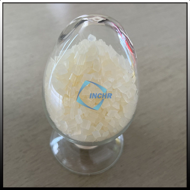
To understand ESD PEEK, we must first look at its base polymer, PEEK. Polyether Ether Ketone is a high-performance thermoplastic known for its incredible mechanical strength, exceptional thermal stability (continuous use up to 250°C/480°F), outstanding chemical resistance, and excellent wear properties. It is often called a “super-engineered plastic.”
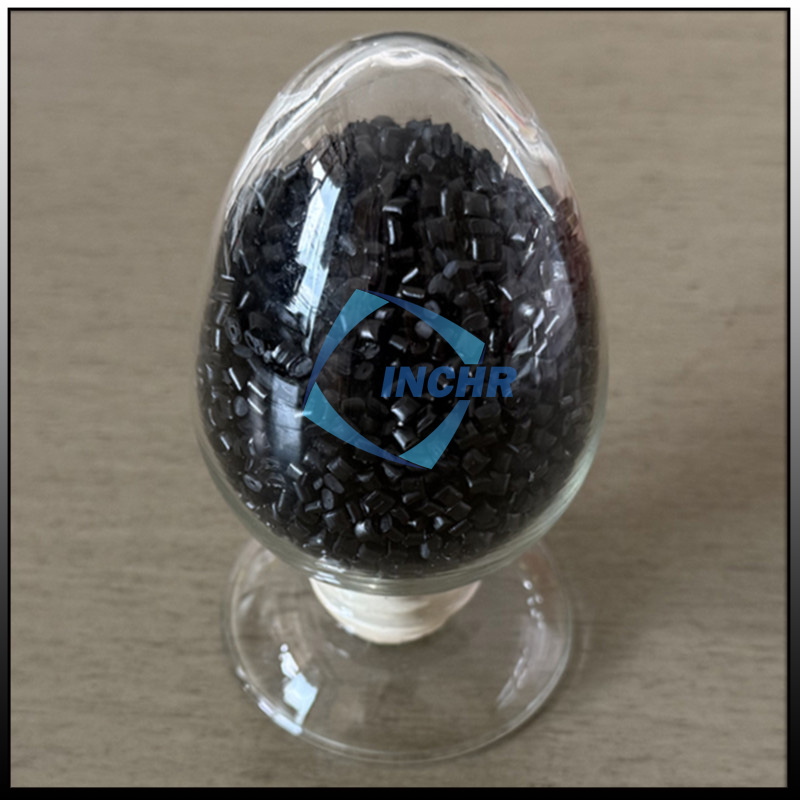
Standard PEEK is an electrical insulator, which means it can easily accumulate static charge—a dangerous trait in an electronics environment. ESD PEEK is created by compounding standard PEEK with conductive fillers, such as carbon nanotubes, carbon fibers, or stainless-steel fibers. This modification transforms the material from an insulator to a static-dissipative one. It does not become conductive; instead, it allows static charges to flow across its surface and dissipate slowly and safely to ground, preventing a sudden discharge that could damage components.
Key Applications of ESD PEEK in the Electronics Field
The unique combination of inherent PEEK properties and ESD safety makes this material a first-choice solution for numerous critical applications.
1. Semiconductor Manufacturing and Handling
The semiconductor fab is a battlefield against contamination and ESD. ESD PEEK is the material of choice for a multitude of handling and processing tools:
Wafer Carriers (Wafer Cassettes/Boat): These carriers hold expensive silicon wafers through numerous fabrication steps. ESD PEEK carriers prevent charge buildup that could attract contaminating particles or zap the delicate circuits on the wafer.
Robotics End-Effectors: Robotic arms used to pick and place wafers, chips, and other components are fitted with grippers made from ESD PEEK. They offer a secure, non-marring, and static-safe grip.
Test Sockets and Burn-In Sockets: These fixtures hold integrated circuits (ICs) during rigorous testing at elevated temperatures. ESD PEEK maintains dimensional stability and provides reliable ESD protection throughout the demanding test cycles.

2. Connectors and Sockets
As data transfer speeds skyrocket with technologies like 5G and IoT, signal integrity in connectors is paramount. ESD PEEK is used for the insulator bodies in high-speed, high-frequency connectors. Its excellent dielectric properties ensure minimal signal loss, while its ESD capability protects the pins from damage during mating and unmating.
3. Automation and Robotics (Cobots)
The rise of collaborative robots (cobots) working alongside humans in assembly lines has increased the need for safe, lightweight, and durable components. ESD PEEK is ideal for gears, bearings, and structural parts within these robots. It ensures they can operate in ESD-protected areas (EPAs) without generating static, while its self-lubricating properties reduce maintenance needs. For more on advanced manufacturing materials, the IEEE Spectrum often publishes relevant articles.
4. Printed Circuit Board (PCB) Testing and Fabrication
Fixture plates for In-Circuit Test (ICT) and Flying Probe Testers are often machined from ESD PEEK. Its rigidity ensures precise alignment of test probes with PCB points, and its ESD properties prevent damage to the board under test. Furthermore, guides, rails, and brackets used on PCB assembly lines benefit from the material’s wear resistance and static-dissipative nature.
5. Components for Additive Manufacturing (3D Printing)
With the advent of high-temperature, high-strength 3D printing materials, ESD-safe filaments are in demand. ESD PEEK filament allows for the rapid prototyping and production of custom jigs, fixtures, and tooling for electronics assembly that are both lightweight and ESD-compliant, directly on the factory floor.
The Future and Advantages Over Metals
The trend towards miniaturization and higher performance in electronics will only intensify the need for materials like ESD PEEK. Its advantages are clear when compared to traditional materials like metals:
Lightweight: Significantly lighter than aluminum or stainless steel, reducing inertia in automated equipment and saving energy.
Corrosion Resistance: Impervious to most chemicals and solvents used in cleaning and etching processes, unlike metals that can corrode and particulate.
Non-Marking: Softer than metals, it will not scratch or damage delicate surfaces like gold-plated connectors or silicon wafers.
Processability: Can be easily machined into complex shapes or increasingly 3D printed, allowing for rapid design iterations and custom solutions.
Conclusion
ESD PEEK is far more than just a plastic; it is a critical enabling material that safeguards the very heart of the digital age. By providing a robust combination of static dissipation, extreme durability, and chemical resistance, it ensures the integrity, reliability, and manufacturability of the electronic devices we rely on every day. As technology continues to advance, the role of ESD PEEK as the guardian of sensitive electronics will only become more vital, solidifying its place on the factory floors of today and the innovation hubs of tomorrow.