As semiconductor processes advance to 7nm and beyond, extreme manufacturing environments demand rigorous material performance. Injection molded PEEK (polyether ether ketone), a high-performance engineering plastic, has become an indispensable core material in the semiconductor manufacturing chain due to its comprehensive advantages including high temperature resistance, chemical inertness, dimensional stability and low pollution. It runs through multiple key production processes, effectively improving production yield and reducing operational costs.
In lithography and etching, two core processes requiring ultra-high precision and corrosion resistance, injection molded PEEK’s advantages are particularly prominent. It is widely used in manufacturing wafer positioning fixtures, reticle holders and etching chamber showerheads. With a low coefficient of thermal expansion of 5×10⁻⁵/℃, it maintains micron-level positioning accuracy even when temperature fluctuates. Its excellent chemical inertness can resist erosion from photoresists, developers and fluorine-based plasmas. Compared with traditional metal components, PEEK components can reduce particle contamination by more than 90%, avoiding wafer surface damage and ensuring the accuracy of circuit pattern transfer.Semiconductor Lithography Process Material Selection Guide.
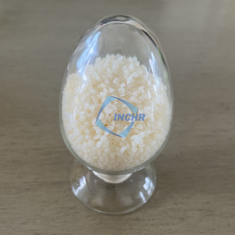
In wafer handling and storage, injection molded PEEK (especially antistatic modified varieties) is the preferred material for core consumables, widely used in Front-Opening Unified Pods (FOUPs), wafer baskets and vacuum nozzles. Its high wear resistance and low particle generation rate can effectively avoid scratches and contamination during wafer transfer. The low outgassing property maintains the cleanliness of the reticle storage environment, which is crucial for EUV lithography technology requiring ultra-high cleanliness. Meanwhile, dimensional stability under temperature changes prevents wafer damage caused by carrier deformation. Performance Parameters of Antistatic Injection Molded PEEK Materials.
In the testing and packaging stage, components such as test sockets and packaging molds made of injection molded PEEK significantly improve process reliability. Its long-term service temperature of up to 260℃ can adapt to high-temperature testing environments, and its excellent electrical insulation ensures stable signal transmission during high-frequency testing. Compared with metal molds, PEEK molds have an elastic modulus close to that of silicon wafers, which can reduce chip cracking caused by thermal stress and increase packaging yield by 5%-10%.
Environmental advantages further broaden the application prospects of injection molded PEEK. This 100% recyclable material has minimal performance loss after multiple heat treatments, aligning with the semiconductor industry’s green manufacturing trend. With continuous process upgrades, modified injection molded PEEK materials such as graphene-reinforced varieties are constantly expanding application boundaries, providing stronger material support for high-end chip manufacturing.