In the highly precise world of semiconductor manufacturing, every component must meet rigorous standards for performance, reliability, and cleanliness. One such critical component is the ESD PEEK board, specifically designed for wafer carriers. These boards play a vital role in safeguarding delicate wafers during storage, transport, and processing.
What is ESD PEEK?
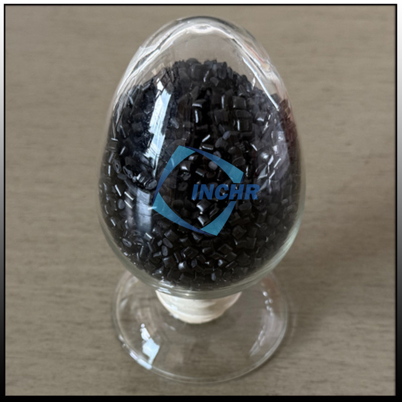
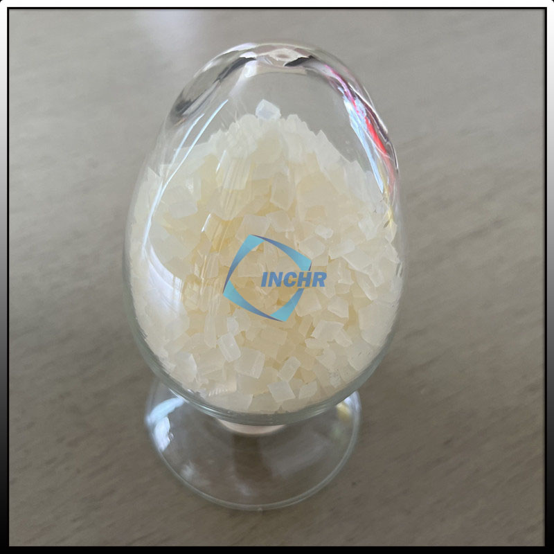
PEEK (Polyether Ether Ketone) is a high-performance thermoplastic known for its exceptional mechanical strength, chemical resistance, and thermal stability. When combined with electrostatic discharge (ESD) properties, it becomes an ideal material for semiconductor applications. ESD PEEK boards prevent static buildup, which could otherwise damage sensitive wafers.
Why ESD PEEK Boards Are Essential
Static Control: Semiconductor wafers are extremely vulnerable to electrostatic discharge. It boards dissipate static electricity, reducing the risk of damage to microchips.
Durability: PEEK maintains its integrity under high temperatures and harsh chemical environments, making it suitable for repeated use in cleanrooms.
Cleanroom Compatibility: The material generates minimal particles, ensuring it meets ISO Class 1 cleanroom standards.
Applications in Wafer Carriers
Wafer carriers, such as Front Opening Unified Pods (FOUPs) and cassettes, rely on ESD PEEK boards to provide a secure, static-safe environment. These boards are often used as support plates or dividers within carriers, ensuring wafers remain aligned and protected.

Industry Standards and Advancements
ESD PEEK boards comply with SEMI standards, ensuring compatibility with automated handling systems. Recent advancements focus on enhancing wear resistance and reducing outgassing, further minimizing contamination risks.
For more details on semiconductor materials, check our guide on advanced polymers in electronics.
Conclusion
ESD PEEK boards are indispensable in semiconductor manufacturing, offering unmatched protection for wafer carriers. Their ability to combine static control with durability and cleanliness makes them a cornerstone of modern fab operations.
To learn more about wafer carrier components, visit SEMI.org.