Conductive Compounds for 3D Printing: Powering the Next Wave of Innovation
3D printing has evolved from producing simple prototypes to manufacturing complex, functional parts. A significant driver of this evolution is the development of advanced materials, particularly conductive compounds. These specialty filaments and resins are transforming how we design and integrate electronics, opening doors to innovations that were once the realm of science fiction.
What Are Conductive Compounds?
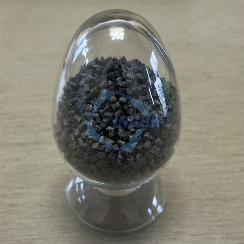
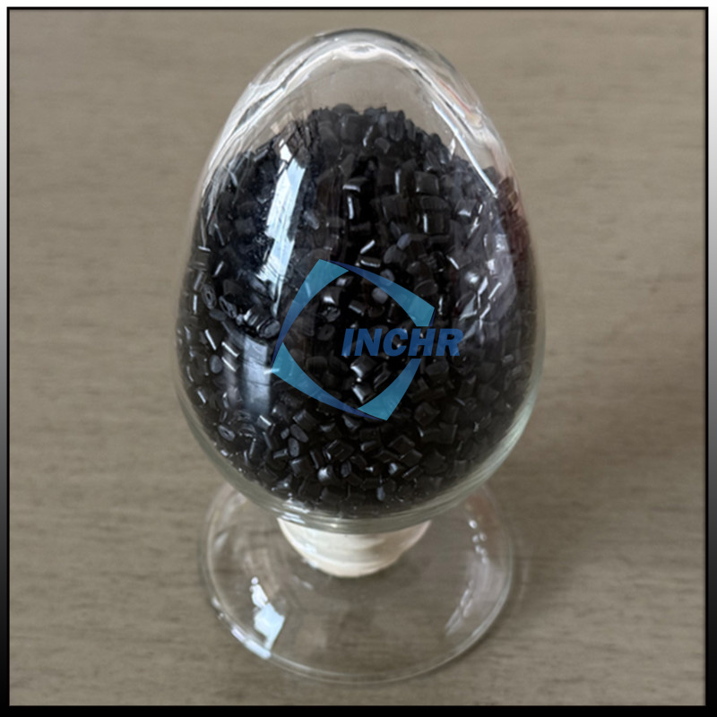
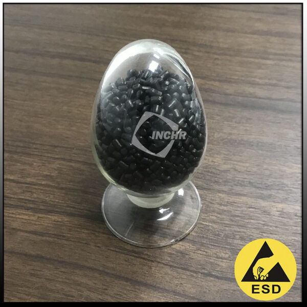
Conductive compounds for 3D printing are materials infused with electrically conductive elements. The most common base material is thermoplastics like PLA or ABS, which are mixed with conductive additives such as:
Carbon-Based Fillers: This includes carbon black, carbon nanotubes, and graphene. These are popular for achieving moderate conductivity while maintaining good printability.
Metal Fillers: Finely powdered copper, silver, or stainless steel are mixed into a polymer binder. These compounds often offer higher conductivity but can be more challenging to print.
The result is a filament or resin that can carry an electrical current, allowing you to 3D print circuits, sensors, and other functional electronic components directly into a structure.
Key Applications and Breakthroughs
The ability to print conductive paths unlocks a vast array of applications across industries:
Embedded Electronics and Sensors: Imagine 3D printing a drone arm with wiring printed directly inside it, reducing weight and assembly parts. Or creating a custom medical device with touch sensors integrated into its handle. This is the promise of conductive printing, enabling more robust and compact designs.
Rapid Prototyping (PCB Alternatives): Engineers and designers can use conductive filament to quickly print and test circuit board layouts, touch interfaces, and simple switches directly on their desktop 3D printer. This drastically accelerates the product development cycle.
Wearable Technology: Conductive composites are ideal for flexible, wearable devices. From smart clothing with integrated biometric sensors to personalized wearable electrodes, these materials provide the necessary flexibility and functionality.
Aerospace and Automotive: The weight-saving potential is crucial here. Printing conductive elements within structural components can simplify wiring harnesses and reduce overall vehicle mass, a critical factor for efficiency, as seen in research from institutions like NASA.
Advantages Over Traditional Methods
Why use 3D printing for electronics instead of traditional PCB manufacturing?
Design Freedom: Create circuits in three dimensions, on curved surfaces, and in geometries impossible for flat boards.
Complex Integration: Print electronics directly into structural components, reducing assembly steps and potential failure points.
Rapid Iteration: Test and modify designs in hours, not weeks.
Customization: Easily produce one-off, highly customized devices cost-effectively.

Challenges and The Road Ahead
While promising, the technology is still maturing. Conductivity of printed traces is generally lower than that of copper, and resolution can be coarse compared to etched circuits. However, ongoing research into new composite materials and hybrid printing systems is rapidly closing this gap.
The future is bright for conductive 3D printing. As materials improve and printers become more advanced, we will move closer to a reality where complex electronic devices are printed whole, seamlessly merging form and function.