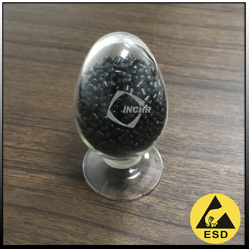
Introduction of PEEK ESD
PEEK ESD compound is a high-performance material made by combining polyetheretherketone (PEEK) with antistatic functional materials. PEEK ESD compound has antistatic properties, and its surface resistivity is within a specific range (usually 10⁶-10⁹Ω/square), which can effectively conduct the generated static electricity and prevent the accumulation and discharge of static electricity. While it has an antistatic function, the PEEK ESD compound still maintains the high strength, high heat resistance, chemical corrosion resistance, and other characteristics of the PEEK material itself
Application of PEEK ESD for electronic equipment parts manufacturing field
Used for integrated circuit packaging components and electronic connectors: In the packaging process of integrated circuits, the requirements for electrostatic protection are extremely high. PEEK ESD compound can be used to print packaging brackets, sockets, and other components, which can not only provide good mechanical support and protection but also effectively prevent static electricity from damaging sensitive integrated circuit chips. For example, in the packaging of high-end chips, parts printed with PEEK ESD compound can ensure the safety of chips during transportation, storage, and use. Electronic connectors need to have good conductivity and antistatic properties to ensure the stability of signal transmission. PEEK ESD compound can print electronic connectors of various shapes and sizes to meet the connection requirements of different electronic devices.
Application of PEEK ESD for semiconductor manufacturing auxiliary materials
Used for wafer carriers and mask-related parts in photolithography processes: In the semiconductor manufacturing process, wafer carriers, such as front-opening wafer transfer boxes (FOUPs) and wafer baskets, are required for the transportation and storage of wafers. PEEK ESD compound has good wear resistance, chemical resistance, dimensional stability, and antistatic properties, and is very suitable for the manufacture of wafer carriers. It can reduce the wear and electrostatic damage of wafers during transportation and storage, and improve the production efficiency and quality of wafers. The photolithography process is one of the key links in semiconductor manufacturing, and the cleanliness and precision of the mask are extremely high. PEEK ESD compounds have the characteristics of high hardness, few particles, high cleanliness, and anti-static. They can be used for printing the support, fixture, and other parts of the mask, providing stable support and protection for the mask while preventing static electricity from causing pollution and damage to the mask.
Application of PEEK ESD for the medical field
Used for orthopedic implants and medical device shells: PEEK material itself has good biocompatibility and elastic modulus similar to human bone, making it an ideal orthopedic implant material. On this basis, PEEK ESD compounds have added antistatic properties, which can reduce the discomfort and potential risks of implants in the human body caused by static electricity. For example, 3D-printed PEEK ESD compounds intervertebral fusion devices, artificial joints, and other orthopedic implants can better meet the treatment needs of patients. Some medical devices have high requirements for electrostatic protection, such as pacemakers and defibrillators. PEEK ESD compound can be used to print the shell of these medical devices, which can provide good mechanical protection and prevent static electricity from interfering with and damaging the electronic components inside the equipment.
Application of PEEK ESD for the aerospace field
Used for aircraft parts and satellite parts. In the aerospace field, aircraft parts need to have high strength, lightweight, and antistatic properties. PEEK ESD compound can be used to manufacture aircraft structural parts, interior parts, connectors, and other parts through 3D printing technology, which can not only reduce the weight of the aircraft and improve fuel efficiency, but also effectively prevent static electricity from interfering with the aircraft’s electronic equipment and communication systems. When satellites are operating in space, they are affected by various radiation and static electricity. PEEK ESD compound has good radiation resistance and antistatic properties and can be used to print satellite antennas, solar panel brackets, and other parts to ensure the normal operation and communication of satellites.
Application of PEEK ESD for mold manufacturing
The high-temperature resistance and antistatic properties of the PEEK ESD compound make it suitable for manufacturing injection molds and die-casting molds. 3D printed PEEK ESD compound injection molds can be used to produce plastic products that are sensitive to static electricity, such as housings for electronic components, plastic packaging, etc. Compared with traditional metal molds, 3D-printed molds have the advantages of a short manufacturing cycle, low cost, and a high degree of customization. In the die-casting process, the mold needs to withstand high temperature, high pressure, and high-speed impact of molten metal. The high strength and high-temperature resistance of PEEK ESD compound materials make it possible to print key components such as cores and cavities of die-casting molds, thereby improving the service life and production efficiency of the molds.