The semiconductor industry demands extreme precision, unmatched cleanliness, and rigorous static control. Even a minute electrostatic discharge (ESD) can irrevocably damage delicate microchips and circuitry, leading to massive yield losses. This is where Electrostatically Dissipative Polyether Ether Ketone (ESD PEEK) emerges as a critical material, engineered to meet the stringent requirements of modern semiconductor fabrication.

The Critical Need for ESD Control
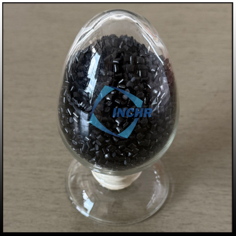
Electrostatic discharge is a pervasive threat in semiconductor facilities. As components become smaller and more powerful, their susceptibility to ESD increases. Traditional insulative plastics, like standard PEEK, can accumulate dangerous charges through friction (tribocharging). ESD PEEK is specially formulated to mitigate this risk. By incorporating conductive fillers like carbon nanotubes or carbon fibers, it gains a consistent surface resistivity typically in the range of 10^6 to 10^9 Ω/sq. This allows charges to dissipate safely and gradually, preventing sudden discharges that can destroy sensitive components.
Learn more about our range of high-performance ESD Plastics for Semiconductor Applications.
Unmatched Performance in Harsh Environments
Semiconductor manufacturing involves aggressive chemicals, high temperatures, and repeated sterilization. ESD PEEK excels here where other ESD plastics fail.
Chemical Resistance: It withstands prolonged exposure to harsh solvents, acids, and plasmas used in etching and cleaning processes, ensuring long-term part integrity without degradation.
Thermal Stability: With a continuous service temperature often exceeding 250°C, ESD PEEK is ideal for high-temperature applications like wafer handling near deposition or oxidation furnaces.
Mechanical Strength: It retains the excellent mechanical properties of virgin PEEK, offering high wear resistance, stiffness, and low particle generation, which is vital for maintaining ultra-clean environments.
Key Applications in Semiconductor Fabrication
ESD PEEK is the material of choice for components that directly handle or are in proximity to wafers and chips:
Wafer Carriers and Cassettes: These transport and store wafers throughout the production process. ESD PEEK prevents charge buildup that could attract contaminants or cause arcing.
Robotics and Automation: End-effectors, grippers, and gears made from ESD PEEK ensure safe, clean, and reliable handling of silicon wafers without causing mechanical or electrical damage.
Test Sockets and Burn-In Sockets: These components require precise, reliable electrical contact without static buildup that could interfere with testing or damage the device.
Process Tool Components: Used in parts within lithography, etching, and ion implantation equipment where ESD protection is paramount.
Understand ESD standards and protocols from the ESD Association.
Advantages Over Alternative Materials
While other materials like static-dissipative plastics or coatings exist, ESD PEEK offers a unique combination of benefits:
Inherent Property: The ESD property is bulk-modified, meaning it won’t wear off or wash away like topical coatings, ensuring permanent protection.
Ultra-Low Contamination: Its low outgassing and minimal particle shedding are crucial for maintaining high yields in cleanrooms.
Durability: Components last significantly longer than those made from less robust ESD materials, reducing downtime and maintenance costs.
The Future of Semiconductor Manufacturing with ESD PEEK
As the industry advances towards smaller nodes and more complex 3D architectures, the tolerance for ESD damage and contamination shrinks to zero. ESD PEEK will continue to be foundational in developing next-generation manufacturing equipment, enabling the production of more powerful and efficient electronic devices. Ongoing material science innovations aim to enhance its properties further, making it even more effective and indispensable.
Conclusion
In the high-stakes world of semiconductor manufacturing, ESD PEEK provides an essential blend of static dissipation, exceptional durability, and unparalleled cleanliness. It is not just a material; it is a enabling technology that safeguards multi-million dollar production lines and drives innovation forward, ensuring the reliable production of the chips that power our modern world.