2024-03-28
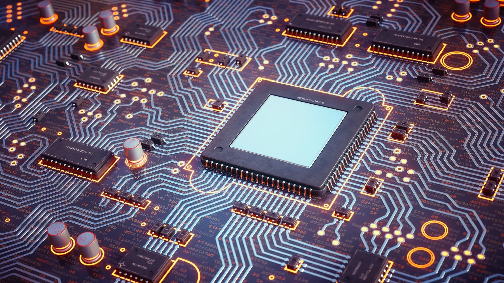
As the demand for chips continues to increase in various fields such as communication equipment, consumer electronics, and automobiles, the global chip shortage is intensifying. The chip manufacturing process is very complex. In terms of semiconductor manufacturing, silicon wafers, electronic specialty gases, masks, photoresists, targets, chemicals and other materials and related equipment tend to receive more attention. Few people introduce plastic materials that goes throughout the entire semiconductor manufacturing process.
The biggest challenge facing semiconductor manufacturing is the control of pollution. Especially with the development of semiconductor technology, electronic components are getting smaller and more complex, the tolerance for impurities is getting lower and lower, and the production conditions are becoming more and more difficult. The more demanding. Dust removal, high temperature, highly corrosive chemicals, etc.In the entire semiconductor manufacturing process, the main role of plastic is packaging and transmission, connecting various processing processes, preventing contamination and damage, optimizing pollution control, and improving the yield of key semiconductor manufacturing processes. The plastic materials used include PEEK, PPS, PP, ABS, PVC, PBT, PC, fluoroplastics, PAI, COP, etc. With the continuous development of semiconductor technology, the performance requirements for materials are getting higher and higher.
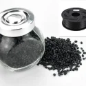
Let’s focuse on the application of special engineering plastic ESD PEEK CNT in semiconductor manufacturing.
- CMP Fixed Ring
Chemical mechanical polishing (CMP) is a key process technology in the wafer production process. During the grinding process, a CMP retaining ring is used to fix the silicon wafer and silicon wafer. The selected materials should have good wear resistance, dimensional stability, chemical corrosion resistance, easy processing, and avoid scratches and contamination of the silicon wafer/circle surface.
The CMP retaining ring is used to secure the chip during grinding. The material chosen should avoid scratches and contamination of the chip surface. It is usually made of standard polyphenylene sulfide.
ESD PEEK CNT has high dimensional stability, easy processability, good mechanical properties, good chemical resistance and good wear resistance. Compared with PPS or PEI rings, CMP retaining rings made of PEEK have stronger wear resistance and double the service life, thereby reducing downtime and increasing chip production.
- Wafer Carrier
Wafer carriers, as the name suggests, are used to load wafers, including wafer carrier boxes, wafer transfer boxes and wafer boats. The time that wafers are stored in shipping boxes accounts for a large portion of the entire production process, and the materials, quality, and cleanliness of the wafer box itself may have a greater or lesser impact on wafer quality.
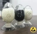
Wafer carriers generally use materials that are resistant to high temperatures, have excellent mechanical properties, dimensional stability, durability, antistatic, low outgassing, low precipitation and are recyclable. ESD PEEK CNT can be used to manufacture carriers for general transport processes. Generally use antistatic PEEK. PEEK has many excellent properties, such as abrasion resistance, chemical resistance, dimensional stability, antistatic properties and low outgassing, which help prevent particle contamination. and improve the reliability of chip processing, storage and transfer.Suitable plastics include: PEEK, PFA, PP, PES, PC, PEI, COP, etc., generally after antistatic modification.
- Mask Box
A photomask is a pattern master used in the photolithography process in chip manufacturing. It uses quartz glass as a base and is coated with chromium metal to block light. Using the exposure principle, the light source is projected onto the silicon wafer through a photomask to expose and display specific patterns. Any dust or scratches attached to the photomask will degrade the quality of the projected image. Therefore, it is necessary to avoid contamination of the photomask and prevent particles generated by collision or friction from affecting the cleanliness of the photomask.
To avoid damage to photomasks due to fogging, friction, or displacement, photomask pods are generally made of antistatic, low-outgassing, and durable materials.
ESD PEEK CNT has the characteristics of high hardness, minimal particle generation, high cleanliness, antistatic, chemical resistance, wear resistance, hydrolysis resistance, good dielectric strength and good radiation resistance. As well as during reticle processing, reticle chips can be stored in a low outgassing and low ionic contamination environment.
- Wafer Tools
Tools used to clamp wafers or silicon wafers, such as wafer clamps, vacuum suction pens, etc. When clamping the wafer, the materials used will not scratch the wafer surface and leave no residue, ensuring the integrity of the wafer surface. Cleanliness.
ESD PEEK CNT has the characteristics of high temperature resistance, wear resistance, good dimensional stability, low outgassing rate, and good hygroscopicity. When using PEEK wafer clamps to clamp wafers and silicon wafers, there will be no scratches on the surface of the wafer or silicon wafer. Scratches do not leave residue on wafers and wafers due to friction, thereby improving surface cleanliness of wafers and wafers.
- Semiconductor Packaging Test Socket
A test socket is a device that electrically connects each semiconductor component's direct circuit to the test instrument. Different test sockets are used to test various microchips specific to the integrated circuit designer. The materials used for test sockets should meet the requirements of good dimensional stability, high mechanical strength, less particle formation, good durability, wide temperature range, and easy processing.